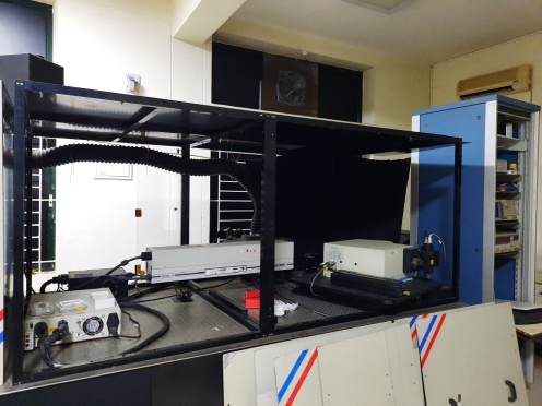
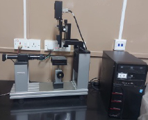
Facilities
The Materials Research Center is well served with equipment for processing and characterization of the materials. The equipment listed could either be central facilities (marked CF) or associated with the laboratories of individual faculty members. {N. Ravishankar, Karuna Kar Nanda, Bikramjit Basu, Abhishek Singh, Balram Sahoo, Prabeer Barpanda, Subinoy Rana, Pachaiyappan Rajamalli, Sujit Das}. Apart from departmental facilities the students also have access to institute and national facilities such as the characterization facilities in the Institute Nano-Science Initiative.
Bath sonicator
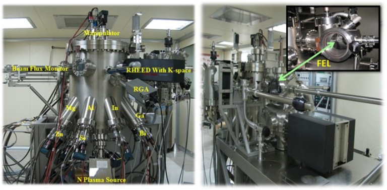
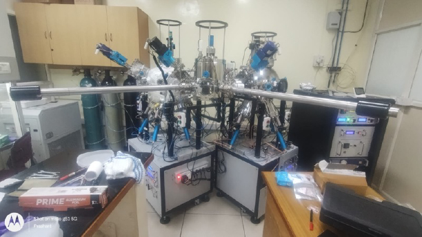
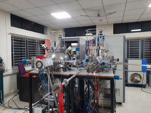
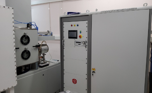
Molecular beam epitaxy (MBE) growth of nitride semiconductors
Pulsed-Laser Deposition Systems (Ch-IB)
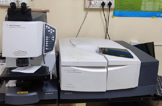
FTIR fitted with optical microscope
Metal and Oxide Sputtering tool shared with Material Engineering department
Atomic Force Microscopes-II VECCO capable of AFM, PFM studies
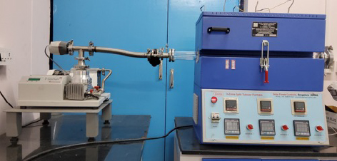
Tubular furnace
DC and RF Sputtering
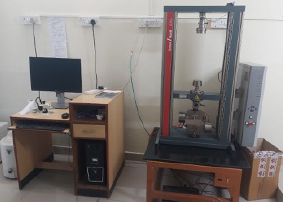
universal tensile testing machine
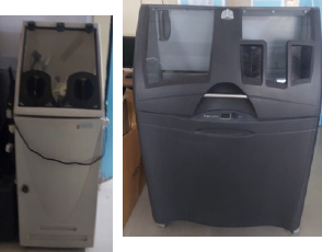
3D printers
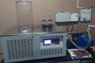
lyophilizer machine
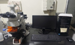
fluorescence microscope
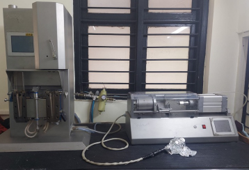
Melt compounder and injection molding machine
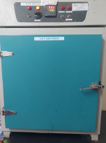
Hot air oven
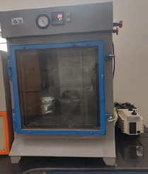
Vacuum oven
Thermal evaporator
Chew simulator
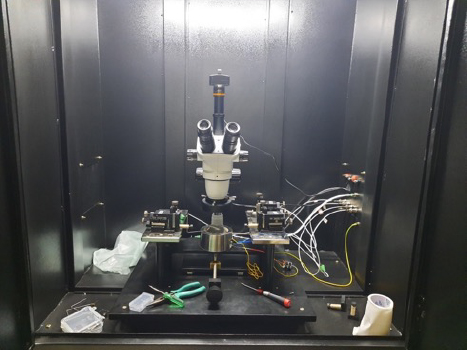
High Temperature probe station-I
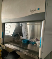
Bio safety cabinet
Photoluminescent measurement setup
Contact angle goniometer
High vacuum sublimation
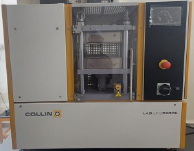
Compression molding machine
OLED measurement set-up
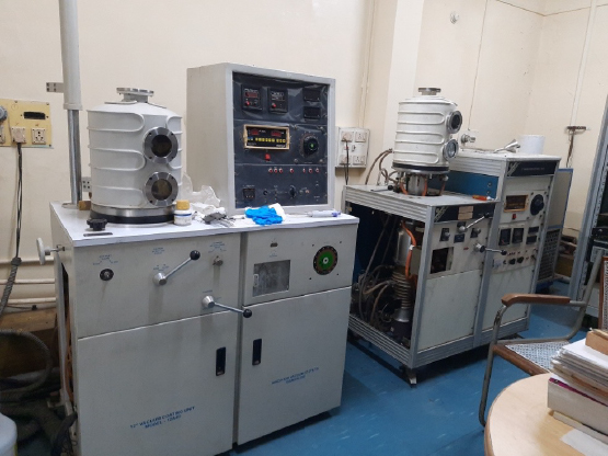
Thermal (right) and E-beam (left) deposition
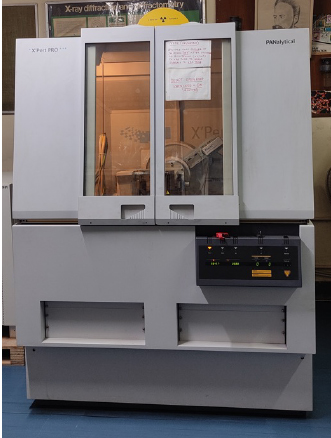
2-Panalytical
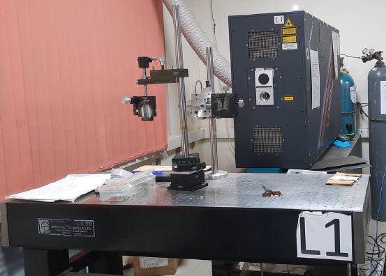
Excimer Lasers (L-I)
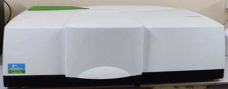
UV Spectrophotometer
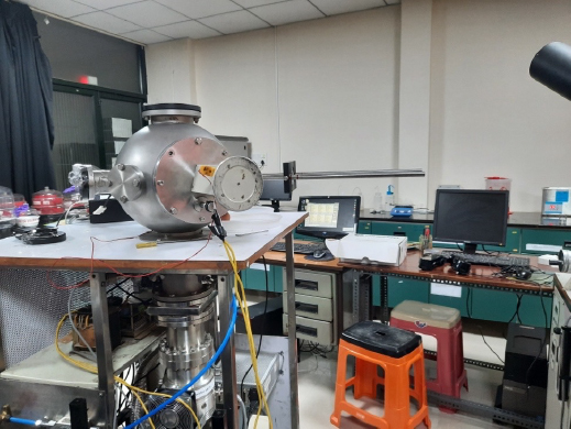
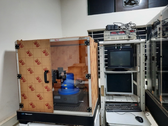
RHEED-assisted Pulsed Laser Deposition (Ch-IA)
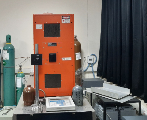
Excimer Lasers (L-II)
Probe sonicator
Incubator
Metal Sputtering
3-Thermo-gravimetric
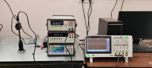
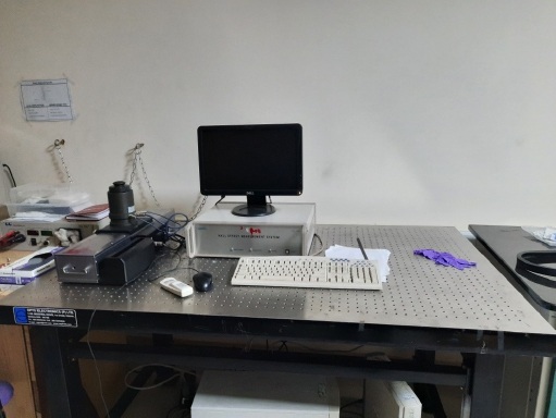
Photodetection measurement system
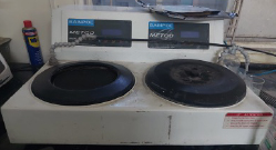
Polishing machine
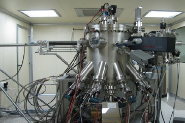
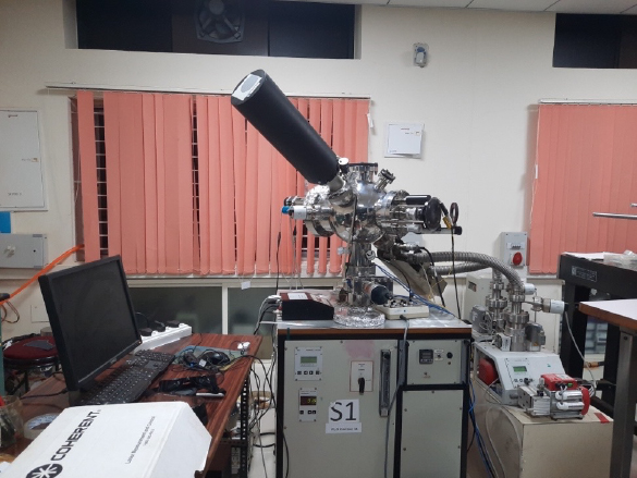
MBE
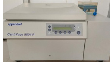
centrifuge machine
X-ray diffractometer (Bruker)
Hall measurement system